Contents
Technical Support
QFN/DFN Application Note
1 Purpose
- This document provides guideline for printed circuit board (PCB) designs for QFN/DFN package.
2 Scope
- The Application Note is written generically for providing guideline for PCB designs to encompass
various QFN/DFN package. 3 Product Description
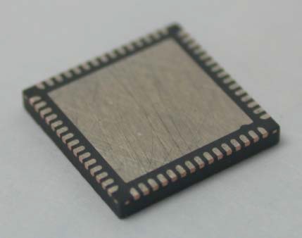
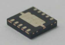
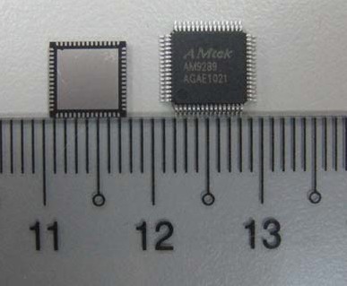
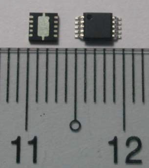
QFN(Quad Flat No-lead)/DFN (Dual Flat No-lead) is a near CSP(Chip Size Package)plastic encapsulated package using conventional copper leadframe technology. The package structure conducts a cost-effective packaging solution that benefits to minimize package size as well as enhances thermal and electrical performance over the traditional leaded packages, as shown in Fig. 1&Fig. 2.
-
Fig. 1: QFN(Quad Flat No-lead) is a package with leads located at the bottom of the package in which leads are arranged in quad side of the package.
-
Fig. 2: DFN(Dual Flat No-lead) is a package with leads located at the bottom of the package in which leads are arranged in dual side of the package.
The QFN/DFN is a leadless surface mount plastic package in which leads located at the bottom of the package instead of the conventional formed peripherally .Thus, a very compact size of the package and a minimum foot print area of PCB were obtained.
As shown in Fig. 3 and Fig.4.
-
Fig.3: The foot print ratio of QFN7x7 over LQFQ7X7 is 60.4%.
-
FFig.4: The foot print ratio of DFN3x3 over MSOP is 61.2%.
The exposed die paddle on the bottom of package efficiently conducts the heat generated from the chip to the PCB and provides a stable grounding electrical connection to the PCB as well, thereby the thermal and electrical properties of the package were enhanced obviously. Further, Instead leads extending peripherally, the QFN/DFN’s leads are disposed at the bottom of the package thereon, as such , the occurrence of leads damage during manufacturing is avoided , a stable cosmetic quality of the package is thus obtained .
Accordingly, QFN/DFN has become the main stream in the leaded packages due to its excellent thermal and electrical performance as well as compact in size, weight & thickness.-
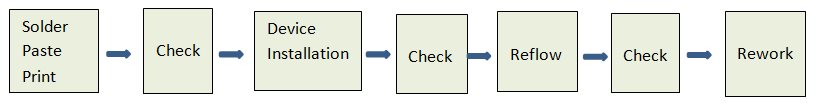
4 Designing the PCB’s
Special care must be taken while the PCB is being designed to ensure the reliable solder joints between the QFN/DFN and the PCB. A number of factors may have a significant effect on soldering QFN/DFN to the PCB. Some of these factors include solder coverage in finger pad
and thermal pad, stencil design ,thermal via’s type...,etc. It should be realized that this is just a guideline to be provided for helping the user in developing her proper PCB during layout design.
Certainly, the package dimensions under discussion are based on the nominal value .
4.1 Designing the finger pad
4.1.1 NSMD: Non-Solder Mask Defined
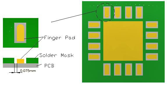
There are two approaches in PCB pad designs, namely Non-Solder Mask Defined Pad(NSMD) and Solder mask Defined Pad (SMD). The NSMD has an opening that is larger than the size of copper pad. Generally, The solder pad area of NSMD is controlled by the size of the copper pad. Moreover, The clearance between the copper pad and solder mask will be 0.075mm typically, as shown in Fig.5. Consequently, the solder is being allowed to anchor to the side of copper pad thus a robustness of solder joint is obtained. Further, Since copper pad etching process is rather stable, a smaller copper pad size can be defined accurately, Accordingly, NSMD pads are preferable for finger pad.-
-
4.1.2 The Opening of the Finger Pads with different lead pitches a.) In the case that the lead pitch ≥ 0.65mm,
Typically, each finger pad have its own solder mask opening with a web of solder mask between two adjacent pads. as shown in Fig. 6.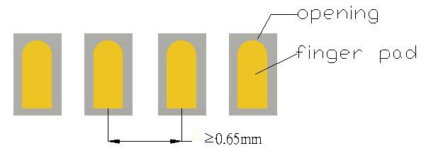
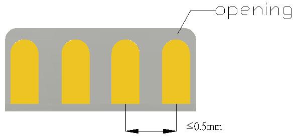
b.) In the case that the lead pitch ≤ 0.5mm,
Since the web has to be at least 0.075mm in width for solder mask to stick to the PCB surface firmly, Accordingly, for the lead pitch ≤ 0.5mm , there is not enough space available for solder mask web in between the pads. Thereby, a “Trench” type solder mask opening in which a big opening is disposed around all pads is being recommended. Further, the corner of inner edge of the solder mask should be rounded to avoid solder bridging from occurring therebetween .as shown in Fig. 7. -
4.1.3 The size of the finger pads
a) The inner edge of the finger pad should be rounded to avoid any solder bridging therebetween.
as shown in Fig. 6 and Fig. 7.
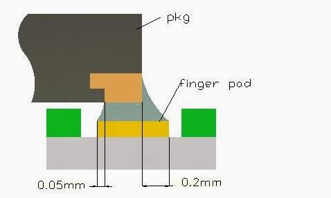
b) For forming a better fillets and accommodating the placement tolerance of pick and place, Generally, the length of finger pad should be longer 0.2mm than the package’s lead and additional 0.05mm extended from the end of inner lead respectively, as shown in Fig. 8.
It should be noted that the formation of the fillet is not guaranteed since the sides of the leads are not plated inherently.c) The width of the finger pad:
c1) in the case that the lead pitch ≥ 0.65mm:
The recommended width is either equal to or a wider 0.05mm(0.025mm per side)than the lead width, as shown in Fig. 9.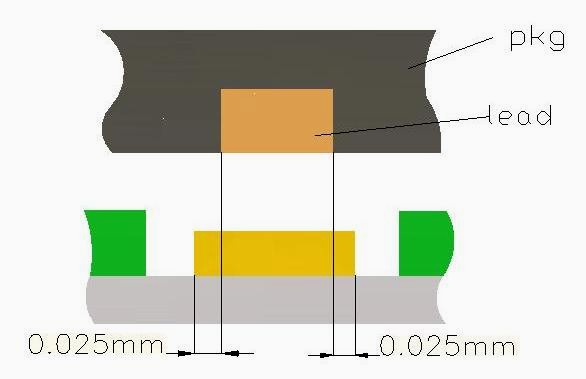
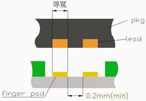
- c2) in the case that the lead pitch ≤ 0.5mm:
The spacing between the finger pads should be kept within a minimum of 0.2mm to avoid the solder bridging therebetween . Consequently, the width of the finger pad should be either equal to or a little smaller than the lead width. Obviously, a wider spacing is beneficial to achieve high SMT yield, as shown in Fig. 10
- c2) in the case that the lead pitch ≤ 0.5mm:
4.2 Designing the thermal pad
4.2.1 SMD: solder mask defined
The pad area was controlled by the size of the solder mask opening, wherein the solder mask opening overlaps the pad land by at least 0.075mm on all four sides. As shown in Fig.11.
In general, the size of the opening should be equal to the exposed pad of the package in order to avoid any solder bridging between thermal pad and perimeter leads. Since the size of pad land is larger than the opening, thus the heat generated from the chip can be conducted effectively from the package. Accordingly, SMD is highly recommended for the design of the thermal pad.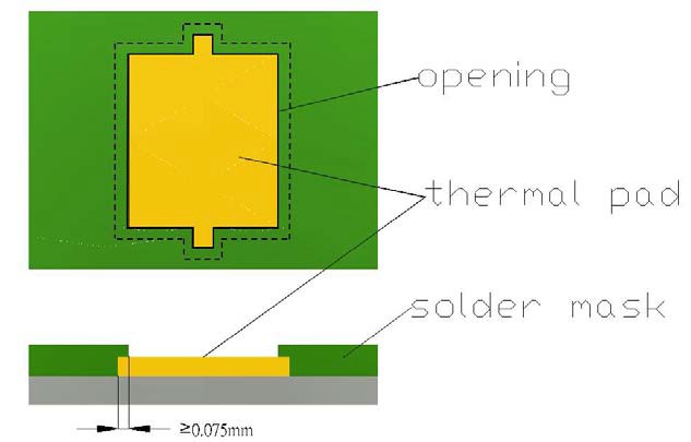
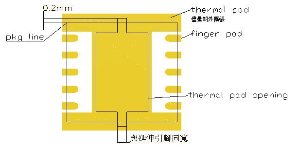
- 4.2.2: A method for an easier check of the solder joint of the exposed pads was provided, wherein a protruded lead is extended from the exposed pad so as to the solder joint between the thermal pad and the exposed pad can be observed easily from the side of the package.
The extended thermal pad opening should be 0.2mm longer than the PKG line in length and equal to lead in width, as shown in Fig. 12.
4.2.3: It’s recommended that always generate as large a thermal pad land as allowable on the top layer of PCB for obtaining a better heat dissipation ,particularly for DFN package with leads on two sides only. as shown in Fig. 12.
4.2.4: In case of an asymmetrical protruded lead is extended from the exposed pad,as shown in Fig.13A. A web ,as shown in Fig13B & 13C, is supposed to be deposited in between the thermal pad and extended opening to avoid a twisted device from occurring.4.2.5: In general, the size of the opening should be equal to the exposed pad of the package, as is depicted in 4.2.1, Adequate spacing between thermal pad and perimeter leads is necessary to prevent solder bridging. Practically, a minimum spacing of 0.2mm is satisfactory for most designs. As shown in Fig.14.
By this constraint, the dimension of thermal pad opening will be determinated by using the following relations:
(A) if (GDmin – D1)/2 ≥ 0.2mm, then the opening is equal to the exposed pad in size;
(B) if (GDmin – D1)/2 < 0.2mm, then the opening should be made smaller to make (A) true
wherein the dimension GDmin is the inside to inside finger pad dimension. And D1 is the thermal pad opening dimension.
4.3 Taking tolerance into account
In order to design a proper pad pattern, tolerance analysis is required on package and PCB dimension. Consequently, ZDmin should accommodate the maximum package length or width ( 0.15mm typ.) plus the recommended 0.2mm extensions .(refer to 4.1.3.b) . Later, is the calculation by using DFN 3x3-10L (find data sheet for details)for an example.
ZDmim=D+0.15mm+2(0.2mm)=3.55mm
--- minimum dimension of the outside to outside finger pad
GDmim=D-2(Lmax)-2(0.05mm)=1.9mm
---minimum dimension of the inside to inside finger pad
Consequently, The spacing between perimeter leads and thermal pad will be
½(GDmim-D1)=½(1.9-1.2)=0.35mm > minimum spacing 0.2mm(refer to 4.2.5.(A))
Thus, the optimized opening for the thermal pad D1th is 1.2mm(D1).
5. Designing the thermal vias
For the using of single layer PCB ,since no thermal vias is being deposited therein ,thus any heat sinking must be accomplished on the top layer entirely. This will typically require to generate
as large a thermal pad land as allowable (refer to 4.2.3)as well as filling all unused area with copper tied to thermal pad land to achieve a better heat dissipation .
Theoretically , the heat conduction paths from the device through the thermal vias underneath the device into the copper plane on the bottom layer are the most efficient paths in the PCB structure for heat dissipating. As such, at least 2-layer PCB with vias (1S1P) is highly recommended for the QFN/DFN applications.
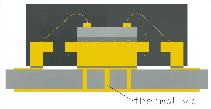
Figure 15
5.1: The size of the thermal via
Practically, the heat would be transferred effectively from the device to the bottom layer of the PCB with a more number of vias and larger vias on the same thermal pad size ,but ,that results in lower package stand-off and solder protrusion due to solder tends to wick down the vias during solder reflow process, thus adversely affecting the strength and reliability of the solder joints.
Accordingly, the following is recommended
Via Pitch: 0.8~1.2mm, and 1.0mm is preferably
Via Dia.: 0.3~0.33m, and 0.3mm is preferably
5.2: The layout of the thermal via
Table 1. provided a suggestion layout of thermal vias for various DFN/QFN packages based on the guidelines depicted above.
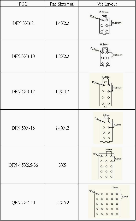
table 1
5.3: The types of the thermal via
A disadvantage of the thermal via is that solder tends to wick down the vias during reflow process, thus results voids being formed in between the exposed pad and the thermal pad. Voids within solder joint underneath the device will have an adverse effect on heat dissipating as well as electrical performance.
Typically, there are 3 different methods employed within industrial for avoid solder wicking from occurring.
- Via plugging method : Theoretically, the vias filled with copper or thermal conductive material was the best ideal structure for heat dissipation. Practically, the cost increase associated with this additional process can be unacceptable for cost-effective design. The plugged vias will prevent solder from wicking into the vias from the top side of the PCB. As shown in Fig.16.
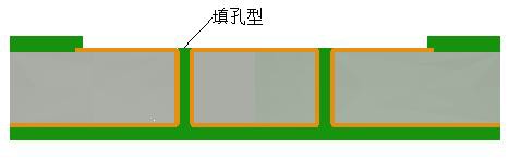
Fig.16
(B)via tenting method : A round-shape of solder mask with a diameter larger 0.1mm than the diameter of via ( i.e. Ø0.4~0.43mm) is placed over the thermal via on the top side of the PCB to prevent solder wicking into the via, as shown in Fig.17.
Practically, the presence of the round-shape solder mask on the top side of the PCB will hinder proper solder paste printing , thus results an uneven solder coverage .As such, voids is likely being formed underneath the device, therefore the thermal performance is adversely being affected
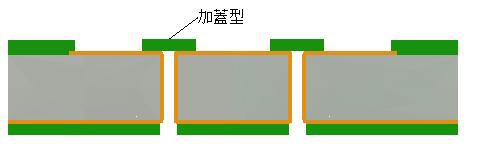
Fig.17
(C) via encroaching method : The solder mask of the bottom side of the PCB is removed to expose a small diameter of copper around each of the thermal vias. As shown in Fig.18. The exposed copper should be normally 0.1mm larger than the diameter of the thermal via in order to restrict the migration of the solder across the bottom plane of the PCB.
The encroached vias allow the solder to wick inside the vias to prevent the voids from being formed. However, it also results in lower stand-off of the package due to solder protruding from the bottom side of the PCB, thus adversely affecting the strength and reliability of the solder joints. This solder protrusion can be avoided by using lower volume of solder paste and reflow peak temperature of less 215°C.
Accordingly, the encroached via is recommended due to less void and better thermal performance while PCB cost not being increased
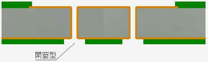
Fig.186. Designing the Screen Print
6.1: Stencil’s thickness & materials
6.1.1:
The thickness of the stencil determines the amount of solder paste deposited onto the PCB land pattern. Due to the fine pitch and small leads geometry of QDF/DFN being used, care must be taken while printing the solder paste on to the PCB .
Too much solder paste will cause solder bridging between the thermal pad under device and the leads on the perimeter of the device, too little solder paste will result in insufficient solder joint and lower stand-off, thus adversely affecting the reliability of the products.6.1.2: Suggested thickness
a.) lead pitch ≤ 0.5mm, Suggested 0.127mm (5mil);
b.) lead pitch ≥ 0.65mm, Suggested 0.150mm (6mil)
Since QFN/DFN are not the only component on the actual application PCB, the above suggested stencil thickness of QFN/DFN may be thinner than other. In such case, a step down stencil is recommended where most of the component has its typical stencil thickness, but the area for the QFN/DFN would be reduce to 5 or 6 mils depending on the QFN/DFN’s lead pitch respectively
6.1.3: The material/making of the stencils
Stencils are usually made of brass or stainless steel, however, stainless steel is more durable and preferable. A Laser-cut or etch , stainless steel is recommended with an electro-polished trapezoidal sidewalls to achieve a more consistent paste release.
6.2: Designing the aperture opening of the finger pad
The area ratio of the aperture opening is critical in order for printing to get good solder paste
release. This is typically accomplished by considering the following two ratio;
a.) Area Ratio = aperture Area/Wall Area = LW/2T(L+W)
b.) Aspect Ratio = aperture width/stencil thickness = W/T
where L and W are the aperture length & width, and T is stencil thickness .
For optimum solder paste release, we recommend:
a.) Area ratio >0.66
b.) Aspect ratio>1.5
Accordingly, It is recommended that the stencil aperture should be 1:1 to finger pad size as both
of the area and aspect ratio are easily achieved by this aperture.
Further, For those spacing with 0.2mm between finger pad and thermal pad , it may be necessary to reduce the stencil aperture length by 20% for avoiding solder bridge from occurring in therebetween.
6.3: Designing the aperture opening of the thermal pad
The large thermal pad being screened with excessive solder may result the device “floating”, thus causing a non-wetting between the QFN/DFN leads and PCB due to solder surface tension during reflow.
It’s, therefore, recommended that a segmented stencil openings should be used instead of one big opening for printing solder paste to the thermal pad.
Accordingly, For exposed pad size < 16mm², a slotted shape opening is recommended. As shown in Fig. 19.
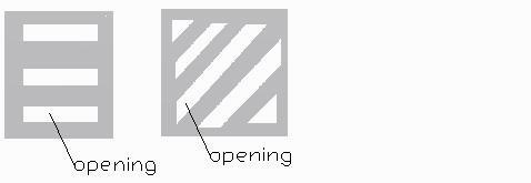
Fig.19
For exposed pad size > 16mm², an array of square or round shape opening is recommended. As In shown in Fig. 20.

Fig.20As such, the stencil opening will be approximately 50% ~ 80% of the thermal pad area, This will typically result in proper solder coverage of the thermal pad with fewer voids and minimizes the occurrence of solder bridging in between the thermal pad and perimeter leads.
Maintaining a web width between opening of 0.3mm minimum is more feasible for the stencil fabrication.
7. Processing SMT
7.1: MSL: Moisture Sensitivity Level
7.1.1: The QFN/DFN is a plastic encapsulated package, the epoxy molding compound (EMC) used for encapsulating tends to absorb moisture from the environment.Usually, the moisture is vaporized instantaneously when temperature rises during reflow, thus the expansion of moisture results in interfacial separation, known as delamination. Moreover, the package bulges once the internal high-pressure vapor is suddenly released from the package, known as “popcorn” effect.
Moisture trapped in the package will induce the effect of popcorn or delamination, thus leads to the failure of the device. Consequently, the MSL rating of QFN/DFN should be recognized in advance prior to SMT.
7.1.2: MSL indicates the floor life of the component after the dry bag is opened.
Table 2 presents the MSL rating respectively as per JEDEC J-STD-020c.
Table 2
MSL-4
MSL-3
MSL-2A
MSL-2
MSL-1Floor Life (after the dry bag is opened)
72 hours
168 hours
192 hours1
Yea r
No Time
LimitComponents , under the environment of ambient temperature less than 30°C and Relative Humidity less than 60%, must be mounted and reflow within the allowable period time (floor life) according to their MSL rating after the original dry bag is opened.
If the components had been exposed to ambient air for a time longer than the specified MSL rating after dry bag being opened, the components are required a pre-baking prior to SMT in order to avoid popcorning from occurring.
7.1.3: Pre-baking
Table 3 depicts the recommended baking time by the different baking temperature and MSL rating respectively.
baking temperature
MSL-4
MSL-3
MSL-2A
MSL-2a.) @ 125℃ 11 hours 9 hours 7 hours 5 hours b.) @ 90℃ 37 hours 33 hours 23 hours 17 hours
table 3
7.2: Typical SMT
 7.2.1 Solder Paste Materials
The QFN/DFN package has essentially low stand-off height. Therefore, post reflow flux cleaning is difficult. Accordingly, a no-clean solder paste is preferred.
7.3: Reflow temperature profile
There are no special considerations necessary when reflowing for QFN/DFN components. Practically, Temperature profile is the most important control in the reflowing process. The actual profile parameters depend upon the solder paste and recommendations from the paste maker should be followed. Further, To maximize the self-alignment effect of the QFN/DFN, It’s recommended that the peak reflow temperature specified for the paste should not be exceeded.
Since the actual profile depends upon the solder paste being used and component density of the PCB, Generally, Amtek does not recommend a specific profile for QFN/DFN.
Instead, for standard eutecdic (Sn/Pb)solder, the profile ramp-up rate of 3 °C /sec or less for preheat, followed by a ramp to peak temperature of profile and finally cool down at a rate no greater than 6 °C /sec is recommended .
Further recommendations, refer to JEDEC/JPC Standard J-STD-20a
7.3.1 QFN/DFN the lead finish materials for QFN/DFN packages
In response to the requirements of today’s Lead(Pb)-free and green components, NiPdAu pre-plated surface finish has been introduced to be an alternative Pb-free solution.
In order to adopt more environmentally friendly materials, Pre-plated leadframe(PPF), wherein a Cu base metal plated with Nickel, followed by Palladium with a thin flushed of Gold, is now being widely used for the leaded package, e.g. QFN/DFN.
Components with NiPdAu pre-plated finishs can withstand much higher reflow temperature than the traditional Sn/Pb finished components. Practically, the reflow peak temperature of PPF finished components needs to be increased more higher than Sn/Pb finished components, besides that, the trends of soldering issue seem to be the same as Sn/Pb finished components.
7.4: The check of solder joints following the reflow process
Unlike traditional leaded packages, the solder joints of QFN/DFN are normally formed underneath the package, Thus, The conventional visual inspection of the solder joints is time consuming undoubtedly. Consequently, X-ray inspection is recommended for verifying any open or short circuit of solder joints after reflow process.
It should be noted that solder non-wetting or solder balling on the peripheral leads is observed frequently while oxidation of the bare Cu on the side of leads is formed under an uncontrolled stored environment. As shown in fig.21.
The solder non-wetting or solder balling phenomenon generally does not present a reliability issue. It ‘s acceptable normally if no further ball-loosing or bridging being found.
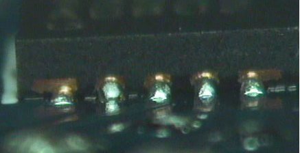
Fig.21
However, It’s possible that a good solder joint of fillets can be obtained if the solder paste contained flux with a superior removal of oxidation is used.
7.5: Rework
Unlike the traditional leaded package, QFN/DFN’s solder joints are not fully exposed outside, As such , rework QFN/DFN packages can be a big challenge due to their small size and thin thickness, Moreover, QFN/DFN will be mounted on a dense PCBs ,thus, the proximity of other component will further complicate the rework due to handling and heating issues..
7.5.1 PreBaking prior to rework
To prevent moisture from inducing popcorn and/or delamination, a prebake consisted
of 125°C for at least 4 hours is highly recommended to remove the residual moisture from PCB & QFN/DFN to avoid the aforementioned failures from occurring prior to rework.
7.5.2 Steps for SMD rework
Generally, QFN/DFN rework are an adaptation of the traditional SMD components while many rework process step ,such as, component removal, site redress, solder paste/flux application, alignment, component placement and reflow have been adopted by industry customarily. As such, further description is hereby omitted.
However, The below two Metcal’s rework solutions may be considered seriously.
(A) Hand soldering : please refer to the application notes of MX-5000 series for details.
(B) Semi automated : please refer to APR-5000’s product details.
Please visit to : http://www.metcal.com, for more information.
-